Explaining the Concept of CPU Die Shrink and Its Benefits

Explaining the Concept of CPU Die Shrink and Its Benefits
The evolution of computer processors has been marked by continuous advancements in technology, one of which is the concept of CPU die shrink. This process has played a crucial role in enhancing the performance, efficiency, and capabilities of modern CPUs. In this article, we will delve into the intricacies of CPU die shrink, its benefits, and its impact on the computing world.
Understanding CPU Die Shrink
What is a CPU Die?
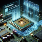
A CPU die is the actual silicon chip that contains the processor’s core components, such as transistors, logic gates, and other circuitry. It is the heart of the CPU, where all the processing tasks are executed. The die is typically housed within a protective package that connects it to the motherboard and other components of a computer system.
What is Die Shrink?
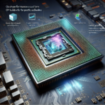
Die shrink refers to the process of reducing the size of the CPU die by using smaller manufacturing processes. This involves shrinking the dimensions of the transistors and other components on the die, allowing more transistors to fit within the same physical space. Die shrink is achieved through advancements in semiconductor fabrication technology, often measured in nanometers (nm).
The Evolution of Die Shrink
The history of die shrink can be traced back to the early days of semiconductor manufacturing. Over the years, the industry has witnessed a steady progression from larger process nodes (e.g., 90nm, 65nm) to smaller ones (e.g., 7nm, 5nm). Each new generation of process nodes brings about significant improvements in performance, power efficiency, and overall capabilities of CPUs.
The Benefits of CPU Die Shrink
Increased Performance
One of the most significant benefits of CPU die shrink is the increase in performance. Smaller transistors can switch on and off more quickly, leading to faster processing speeds. This results in improved overall performance, allowing CPUs to handle more complex tasks and run applications more efficiently.
Enhanced Power Efficiency
Die shrink also contributes to enhanced power efficiency. Smaller transistors require less power to operate, reducing the overall power consumption of the CPU. This is particularly important for mobile devices and laptops, where battery life is a critical factor. Lower power consumption also translates to reduced heat generation, which helps in maintaining optimal operating temperatures.
Higher Transistor Density
As the size of transistors decreases, more transistors can be packed into the same die area. This higher transistor density allows for the integration of more cores, cache memory, and other features within the CPU. The result is a more powerful and versatile processor that can handle a wider range of tasks simultaneously.
Cost Reduction
Die shrink can lead to cost reduction in several ways. Smaller dies require less raw material, which can lower manufacturing costs. Additionally, higher transistor density means that more CPUs can be produced from a single silicon wafer, increasing production efficiency. These cost savings can be passed on to consumers, making advanced CPUs more affordable.
Improved Thermal Management
With smaller transistors generating less heat, die shrink contributes to improved thermal management. This is crucial for maintaining the stability and longevity of the CPU. Efficient thermal management allows for higher clock speeds and better performance without the risk of overheating.
The Challenges of CPU Die Shrink
Manufacturing Complexity
As process nodes become smaller, the complexity of manufacturing increases. Advanced lithography techniques, such as extreme ultraviolet (EUV) lithography, are required to achieve the precision needed for smaller transistors. This adds to the cost and complexity of the manufacturing process.
Quantum Effects
At extremely small scales, quantum effects become more pronounced, leading to challenges such as electron leakage and variability in transistor behavior. These effects can impact the reliability and performance of the CPU, requiring innovative solutions to mitigate their impact.
Design and Verification
Designing and verifying CPUs at smaller process nodes is a complex task. Engineers must ensure that the smaller transistors function correctly and reliably under various conditions. This requires extensive testing and validation, adding to the development time and cost.
Real-World Applications and Impact
Consumer Electronics
Die shrink has had a profound impact on consumer electronics, enabling the development of more powerful and energy-efficient devices. Smartphones, tablets, and laptops have benefited from smaller, more efficient CPUs, leading to improved performance and longer battery life.
Data Centers
In data centers, die shrink has allowed for the deployment of more powerful servers with higher core counts and better energy efficiency. This has led to increased computational capabilities, reduced operational costs, and improved sustainability in data center operations.
Artificial Intelligence and Machine Learning
Die shrink has also played a crucial role in advancing artificial intelligence (AI) and machine learning (ML) technologies. Smaller, more powerful CPUs can handle the complex computations required for AI and ML applications, driving innovation in fields such as autonomous vehicles, natural language processing, and image recognition.
Future Trends in CPU Die Shrink
Continued Process Node Shrinkage
The trend of shrinking process nodes is expected to continue, with manufacturers aiming for even smaller dimensions, such as 3nm and beyond. These advancements will bring about further improvements in performance, power efficiency, and transistor density.
3D Stacking
3D stacking is an emerging technology that involves stacking multiple layers of transistors on top of each other. This approach can further increase transistor density and performance while reducing power consumption. 3D stacking is expected to complement traditional die shrink techniques in the future.
New Materials and Technologies
Researchers are exploring new materials and technologies to overcome the limitations of traditional silicon-based transistors. Materials such as graphene and carbon nanotubes hold promise for creating smaller, faster, and more efficient transistors. These innovations could revolutionize the semiconductor industry and drive the next wave of CPU advancements.
FAQ
What is the primary goal of CPU die shrink?
The primary goal of CPU die shrink is to reduce the size of the transistors and other components on the CPU die. This allows for increased performance, enhanced power efficiency, higher transistor density, and cost reduction.
How does die shrink improve CPU performance?
Die shrink improves CPU performance by allowing smaller transistors to switch on and off more quickly. This results in faster processing speeds and improved overall performance, enabling CPUs to handle more complex tasks efficiently.
What are the challenges associated with die shrink?
The challenges associated with die shrink include increased manufacturing complexity, quantum effects, and the need for extensive design and verification. These challenges require advanced technologies and innovative solutions to overcome.
How does die shrink impact power efficiency?
Die shrink impacts power efficiency by reducing the power required to operate smaller transistors. This leads to lower overall power consumption, reduced heat generation, and improved battery life for mobile devices.
What is the future of CPU die shrink?
The future of CPU die shrink involves continued process node shrinkage, the adoption of 3D stacking technologies, and the exploration of new materials and technologies. These advancements will drive further improvements in CPU performance, efficiency, and capabilities.
Conclusion
CPU die shrink is a fundamental concept in the evolution of computer processors. By reducing the size of transistors and other components, die shrink has brought about significant benefits, including increased performance, enhanced power efficiency, higher transistor density, cost reduction, and improved thermal management. Despite the challenges associated with die shrink, ongoing advancements in semiconductor fabrication technology continue to drive innovation in the computing world. As we look to the future, the continued evolution of die shrink, along with emerging technologies such as 3D stacking and new materials, promises to further revolutionize the capabilities of CPUs and shape the future of computing.